Having learned about digital memory devices in
the last chapter, we know that it is possible to store binary data within
solid-state devices. Those storage "cells" within solid-state memory devices
are easily addressed by driving the "address" lines of the device with the
proper binary value(s). Suppose we had a ROM memory circuit written, or
programmed, with certain data, such that the address lines of the ROM served
as inputs and the data lines of the ROM served as outputs, generating the
characteristic response of a particular logic function. Theoretically, we
could program this ROM chip to emulate whatever logic function we wanted
without having to alter any wire connections or gates.
Consider the following example of a 4 x 2 bit ROM memory (a very small
memory!) programmed with the functionality of a half adder:
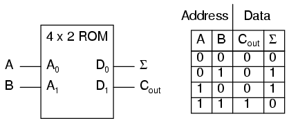
If this ROM has been written with the above data (representing a
half-adder's truth table), driving the A and B address inputs will cause the
respective memory cells in the ROM chip to be enabled, thus outputting the
corresponding data as the Σ (Sum) and Cout bits. Unlike the
half-adder circuit built of gates or relays, this device can be set up to
perform any logic function at all with two inputs and two outputs, not just
the half-adder function. To change the logic function, all we would need to
do is write a different table of data to another ROM chip. We could even use
an EPROM chip which could be re-written at will, giving the ultimate
flexibility in function.
It is vitally important to recognize the significance of this principle
as applied to digital circuitry. Whereas the half-adder built from gates or
relays processes the input bits to arrive at a specific output, the
ROM simply remembers what the outputs should be for any given
combination of inputs. This is not much different from the "times tables"
memorized in grade school: rather than having to calculate the product of 5
times 6 (5 + 5 + 5 + 5 + 5 + 5 = 30), school-children are taught to remember
that 5 x 6 = 30, and then expected to recall this product from memory as
needed. Likewise, rather than the logic function depending on the functional
arrangement of hard-wired gates or relays (hardware), it depends solely on
the data written into the memory (software).
Such a simple application, with definite outputs for every input, is
called a look-up table, because the memory device simply "looks up"
what the output(s) should to be for any given combination of inputs states.
This application of a memory device to perform logical functions is
significant for several reasons:
Software is much easier to change than hardware. Software can be archived on various kinds of memory media (disk,
tape), thus providing an easy way to document and manipulate the function
in a "virtual" form; hardware can only be "archived" abstractly in the
form of some kind of graphical drawing. Software can be copied from one memory device (such as the EPROM chip)
to another, allowing the ability for one device to "learn" its function
from another device. Software such as the logic function example can be designed to perform
functions that would be extremely difficult to emulate with discrete logic
gates (or relays!).
The usefulness of a look-up table becomes more and more evident with
increasing complexity of function. Suppose we wanted to build a 4-bit adder
circuit using a ROM. We'd require a ROM with 8 address lines (two 4-bit
numbers to be added together), plus 4 data lines (for the signed output):
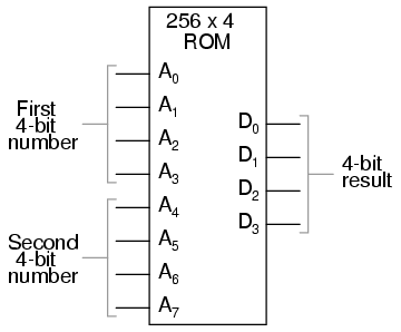
With 256 addressable memory locations in this ROM chip, we would have a
fair amount of programming to do, telling it what binary output to generate
for each and every combination of binary inputs. We would also run the risk
of making a mistake in our programming and have it output an incorrect sum,
if we weren't careful. However, the flexibility of being able to configure
this function (or any function) through software alone generally outweighs
that costs.
Consider some of the advanced functions we could implement with the above
"adder." We know that when we add two sets of numbers in 2's complement
signed notation, we risk having the answer overflow. For instance, if we try
to add 0111 (decimal 7) to 0110 (decimal 6) with only a 4-bit number field,
the answer we'll get is 1001 (decimal -7) instead of the correct value, 13
(7 + 6), which cannot be expressed using 4 signed bits. If we wanted to, we
could avoid the strange answers given in overflow conditions by programming
this look-up table circuit to output something else in conditions where we
know overflow will occur (that is, in any case where the real sum would
exceed +7 or -8). One alternative might be to program the ROM to output the
quantity 0111 (the maximum positive value that can be represented with 4
signed bits), or any other value that we determined to be more appropriate
for the application than the typical overflowed "error" value that a regular
adder circuit would output. It's all up to the programmer to decide what he
or she wants this circuit to do, because we are no longer limited by the
constraints of logic gate functions.
The possibilities don't stop at customized logic functions, either. By
adding more address lines to the 256 x 4 ROM chip, we can expand the look-up
table to include multiple functions:
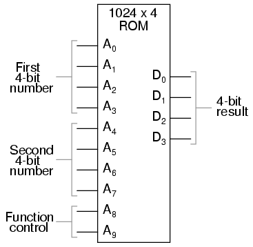
With two more address lines, the ROM chip will have 4 times as many
addresses as before (1024 instead of 256). This ROM could be programmed so
that when A8 and A9 were both low, the output data represented the sum
of the two 4-bit binary numbers input on address lines A0 through A7, just
as we had with the previous 256 x 4 ROM circuit. For the addresses A8=1 and
A9=0, it could be programmed to output the difference (subtraction)
between the first 4-bit binary number (A0 through A3) and the second binary
number (A4 through A7). For the addresses A8=0 and A9=1, we could program
the ROM to output the difference (subtraction) of the two numbers in reverse
order (second - first rather than first - second), and finally, for the
addresses A8=1 and A9=1, the ROM could be programmed to compare the two
inputs and output an indication of equality or inequality. What we will have
then is a device that can perform four different arithmetical operations on
4-bit binary numbers, all by "looking up" the answers programmed into it.
If we had used a ROM chip with more than two additional address lines, we
could program it with a wider variety of functions to perform on the two
4-bit inputs. There are a number of operations peculiar to binary data (such
as parity check or Exclusive-ORing of bits) that we might find useful to
have programmed in such a look-up table.
Devices such as this, which can perform a variety of arithmetical tasks
as dictated by a binary input code, are known as Arithmetic Logic Units
(ALUs), and they comprise one of the essential components of computer
technology. Although modern ALUs are more often constructed from very
complex combinational logic (gate) circuits for reasons of speed, it should
be comforting to know that the exact same functionality may be duplicated
with a "dumb" ROM chip programmed with the appropriate look-up table(s). In
fact, this exact approach was used by IBM engineers in 1959 with the
development of the IBM 1401 and 1620 computers, which used look-up tables to
perform addition, rather than binary adder circuitry. The machine was fondly
known as the "CADET," which stood for "Can't Add, Doesn't
Even Try."
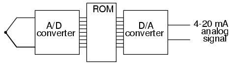
A very common application for look-up table ROMs is in control systems
where a custom mathematical function needs to be represented. Such an
application is found in computer-controlled fuel injection systems for
automobile engines, where the proper air/fuel mixture ratio for efficient
and clean operation changes with several environmental and operational
variables. Tests performed on engines in research laboratories determine
what these ideal ratios are for varying conditions of engine load, ambient
air temperature, and barometric air pressure. The variables are measured
with sensor transducers, their analog outputs converted to digital signals
with A/D circuitry, and those parallel digital signals used as address
inputs to a high-capacity ROM chip programmed to output the optimum digital
value for air/fuel ratio for any of these given conditions.
Sometimes, ROMs are used to provide one-dimensional look-up table
functions, for "correcting" digitized signal values so that they more
accurately represent their real-world significance. An example of such a
device is a thermocouple transmitter, which measures the millivoltage
signal generated by a junction of dissimilar metals and outputs a signal
which is supposed to directly correspond to that junction
temperature. Unfortunately, thermocouple junctions do not have perfectly
linear temperature/voltage responses, and so the raw voltage signal is not
perfectly proportional to temperature. By digitizing the voltage signal (A/D
conversion) and sending that digital value to the address of a ROM
programmed with the necessary correction values, the ROM's programming could
eliminate some of the nonlinearity of the thermocouple's
temperature-to-millivoltage relationship, so that the final output of the
device would be more accurate. The popular instrumentation term for such a
look-up table is a digital characterizer.
Another application for look-up tables is in special code translation. A
128 x 8 ROM, for instance, could be used to translate 7-bit ASCII code to
8-bit EBCDIC code:
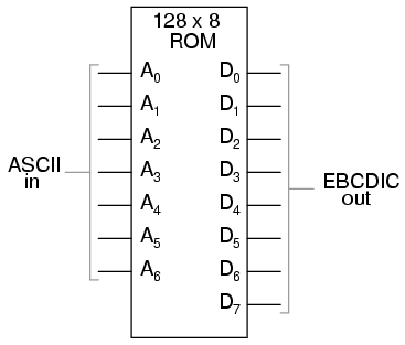
Again, all that is required is for the ROM chip to be properly programmed
with the necessary data so that each valid ASCII input will produce a
corresponding EBCDIC output code. |
