Basic gate function
PARTS AND MATERIALS
-
4011 quad NAND gate (Radio Shack catalog #
276-2411)
-
Eight-position DIP switch (Radio Shack
catalog # 275-1301)
-
Ten-segment bargraph LED (Radio Shack
catalog # 276-081)
-
One 6 volt battery
-
Two 10 kΩ resistors
-
Three 470 Ω resistors
Caution! The 4011 IC is CMOS, and
therefore sensitive to static electricity!
CROSS-REFERENCES
Lessons In Electric Circuits, Volume
4, chapter 3: "Logic Gates"
LEARNING OBJECTIVES
-
Purpose of a "pulldown" resistor
-
How to experimentally determine the truth
table of a gate
-
How to connect logic gates together
-
How to create different logical functions
by using NAND gates
SCHEMATIC DIAGRAM
ILLUSTRATION

INSTRUCTIONS
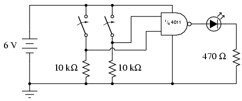
To begin, connect a single NAND gate to two
input switches and one LED, as shown. At first, the use of
an 8-position switch and a 10-segment LED bargraph may seem
excessive, since only two switches and one LED are needed to
show the operation of a single NAND gate. However, the
presence of those extra switches and LEDs make it very
convenient to expand the circuit, and help make the circuit
layout both clean and compact.
It is highly recommended that you have a
datasheet for the 4011 chip available when you build your
circuit. Don't just follow the illustration shown above! It
is important that you develop the skill of reading
datasheets, especially "pinout" diagrams, when connecting IC
terminals to other circuit elements. The datasheet's
connection diagram is an essential piece of information to
have. Shown here is my own rendition of what any 4011
datasheet shows:
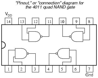
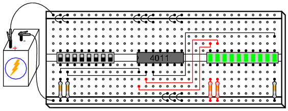
In the breadboard illustration, I've shown
the circuit built using the lower-left NAND gate: pin #'s 1
and 2 are the inputs, and pin #3 is the output. Pin #'s 14
and 7 conduct DC power to all four gate circuits inside the
IC chip, "VDD" representing the positive side of
the power supply (+V), and "Gnd" representing the negative
side of the power supply (-V), or ground. Sometimes the
negative power supply terminal will be labeled "VSS"
instead of "Gnd" on a datasheet, but it means the same
thing.
Digital logic circuitry does not make use of
split power supplies as op-amps do. Like op-amp circuits,
though, ground is still the implicit point of reference for
all voltage measurements. If I were to speak of a "high"
signal being present on a certain pin of the chip, I would
mean that there was full voltage between that pin and the
negative side of the power supply (ground).
Note how all inputs of the unused gates
inside the 4011 chip are connected either to VDD
or ground. This is not a mistake, but an act of intentional
design. Since the 4011 is a CMOS integrated circuit, and
CMOS circuit inputs left unconnected (floating) can
assume any voltage level merely from intercepting a static
electric charge from a nearby object, leaving inputs
floating means that those unused gates may receive any
random combinations of "high" and "low" signals.
Why is this undesirable, if we aren't using
those gates? Who cares what signals they receive, if we are
not doing anything with their outputs? The problem is, if
static voltage signals appear at the gate inputs that are
not fully "high" or fully "low," the gates' internal
transistors may begin to turn on in such a way as to draw
excessive current. At worst, this could lead to damage of
the chip. At best it means excessive power consumption. It
matters little if we choose to connect these unused gate
inputs "high" (VDD) or "low" (ground), so long as
we connect them to one of those two places. In the
breadboard illustration, I show all the top inputs connected
to VDD, and all the bottom inputs (of the unused
gates) connected to ground. This was done merely because
those power supply rail holes were closer and did not
require long jumper wires!
Please note that none of the unused gate
outputs have been connected to VDD or ground,
and for good reason! If I were to do that, I may be forcing
a gate to assume the opposite output state that it's trying
to achieve, which is a complicated way of saying that I
would have created a short-circuit. Imagine a gate that is
supposed to output a "high" logic level (for a NAND gate,
this would be true if any of its inputs were "low"). If such
a gate were to have its output terminal directly connected
to ground, it could never reach a "high" state (being made
electrically common to ground through the jumper wire
connection). Instead, its upper (P-channel) output
transistor would be turned on in vain, sourcing maximum
current to a nonexistent load. This would very likely damage
the gate! Gate output terminals, by their very nature,
generate their own logic levels and never "float" in the
same way that CMOS gate inputs do.
The two 10 kΩ resistors are placed in the
circuit to avoid floating input conditions on the used gate.
With a switch closed, the respective input will be directly
connected to VDD and therefore be "high." With a
switch open, the 10 kΩ "pulldown" resistor provides a
resistive connection to ground, ensuring a secure "low"
state at the gate's input terminal. This way, the input will
not be susceptible to stray static voltages.
With the NAND gate connected to the two
switches and one LED as shown, you are ready to develop a
"truth table" for the NAND gate. Even if you already know
what a NAND gate truth table looks like, this is a good
exercise in experimentation: discovering a circuit's
behavioral principles by induction. Draw a truth table on a
piece of paper like this:
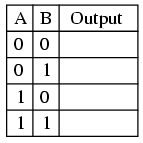
The "A" and "B" columns represent the two
input switches, respectively. When the switch is on, its
state is "high" or 1. When the switch is off, its state is
"low," or 0, as ensured by its pulldown resistor. The gate's
output, of course, is represented by the LED: whether it is
lit (1) or unlit (0). After placing the switches in every
possible combination of states and recording the LED's
status, compare the resulting truth table with what a NAND
gate's truth table should be.
As you can imagine, this breadboard circuit
is not limited to testing NAND gates. Any gate type may be
tested with two switches, two pulldown resistors, and an LED
to indicate output status. Just be sure to double-check the
chip's "pinout" diagram before substituting it pin-for-pin
in place of the 4011. Not all "quad" gate chips have the
same pin assignments!
An improvement you might want to make to
this circuit is to assign a couple of LEDs to indicate input
status, in addition to the one LED assigned to indicate the
output. This makes operation a little more interesting to
observe, and has the further benefit of indicating if a
switch fails to close (or open) by showing the true
input signal to the gate, rather than forcing you to infer
input status from switch position:
|
