|
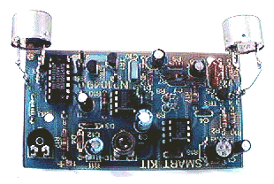
This is a very interesting project with
many practical applications in security and alarm
systems for homes, shops and cars. It consists of a set
of ultrasonic receiver and transmitter which operate at
the same frequency. When something moves in the area
covered by the circuit the circuits fine balance is
disturbed and the alarm is triggered. The circuit is
very sensitive and can be adjusted to reset itself
automatically or to stay triggered till it is reset
manually after an alarm.
As it has already been stated the
circuit consists of an ultrasonic transmitter and a
receiver both of which work at the same frequency. They
use ultrasonic piezoelectric transducers as output and
input devices respectively and their frequency of
operation is determined by the particular devices in
use.
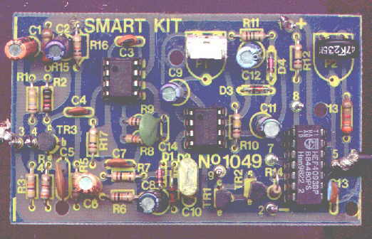
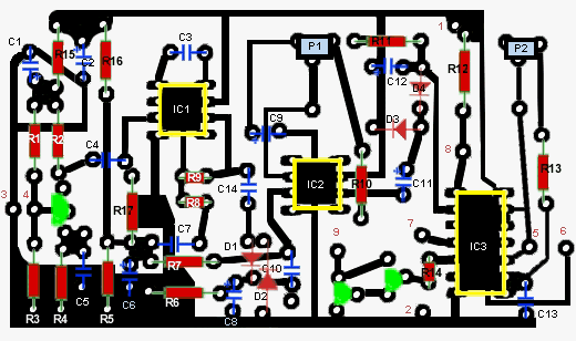
The transmitter is built around two NAND
gates of the four found in IC3 which are used here wired
as inverters and in the particular circuit they form a
multivibrator the output of which drives the transducer.
The trimmer P2 adjusts the output frequency of the
transmitter and for greater efficiency it should be made
the same as the frequency of resonance of the
transducers in use. The receiver similarly uses a
transducer to receive the signals that are reflected
back to it the output of which is amplified by the
transistor TR3, and IC1 which is a 741 op-amp. The
output of IC1 is taken to the non inverting input of IC2
the amplification factor of which is adjusted by means
of P1. The circuit is adjusted in such a way as to stay
in balance as long the same as the output frequency of
the transmitter. If there is some movement in the area
covered by the ultrasonic emission the signal
that is reflected back to the receiver
becomes distorted and the circuit is thrown out of
balance. The output of IC2 changes abruptly and the
Schmitt trigger circuit which is built around the
remaining two gates in IC3 is triggered. This drives the
output transistors TR1,2 which in turn give a signal to
the alarm system or if there is a relay connected to the
circuit, in series with the collector of TR1, it becomes
activated. The circuit works from 9-12 VDC and can be
used with batteries or a power supply.
Click Here to View
Circuits
First of all let us consider a few
basics in building electronic circuits on a printed
circuit board. The board is made of a thin insulating
material clad with a thin layer of conductive copper
that is shaped in such a way as to form the necessary
conductors between the various components of the
circuit. The use of a properly designed printed circuit
board is very desirable as it speeds construction up
considerably and reduces the possibility of making
errors. Smart Kit boards also come pre-drilled and with
the outline of the components and their identification
printed on the component side to make construction
easier. To protect the board during storage from
oxidation and assure it gets to you in perfect condition
the copper is tinned during manufacturing and covered
with a special varnish that protects it from getting
oxidised and also makes soldering easier. Soldering the
components to the board is the only way to build your
circuit and from the way you do it depends greatly your
success or failure. This work is not very difficult and
if you stick to a few rules you should have no problems.
The soldering iron that you use must be light and its
power should not exceed the 25 Watts. The tip should be
fine and must be kept clean at all times. For this
purpose come very handy specially made sponges that are
kept wet and from time to time you can wipe the hot tip
on them to remove all the residues that tend to
accumulate on it. DO NOT file or sandpaper a dirty or
worn out tip. If the tip cannot be cleaned, replace it.
There are many different types of solder in the market
and you should choose a good quality one that contains
the necessary flux in its core, to assure a perfect
joint every time. DO NOT use soldering flux apart from
that which is already included in your solder. Too much
flux can cause many problems and is one of the main
causes of circuit malfunction. If nevertheless you have
to use extra flux, as it is the case when you have to
tin copper wires, clean it very thoroughly after you
finish your work. In order to solder a component
correctly you should do the following:
@Clean the component leads with a small
piece of emery paper.
@Bend them at the correct distance from
the components body and insert the component in its
place on the board.
@You may find sometimes a component with
heavier gauge leads than usual, that are too thick to
enter in the holes of the p.c. board.
@In this case use a mini drill to
enlarge the holes slightly. Do not make the holes too
large as this is going to make soldering difficult
afterwards.
@Take the hot iron and place its tip on
the component lead while holding the end of the solder
wire at the point where the lead emerges from the board.
The iron tip must touch the lead slightly above the p.c.
board.
@When the solder starts to melt and flow
wait till it covers evenly the area around the hole and
the flux boils and gets out from underneath the solder.
The whole operation should not take more than 5 seconds.
Remove the iron and allow the solder to cool naturally
without blowing on it or moving the component. If
everything was done properly the surface of the joint
must have a bright metallic finish and its edges should
be smoothly ended on the component lead and the board
track. If the solder looks dull, cracked, or has the
shape of a blob then you have made a dry joint and you
should remove the solder (with a pump, or a solder wick)
and redo it.
@Take care not to overheat the tracks as
it is very easy to lift them from the board and break
them.
@When you are soldering a sensitive
component it is good practice to hold the lead from the
component side of the board with a pair of long-nose
pliers to divert any heat that could possibly damage the
component.
@Make sure that you do not use more
solder than it is necessary as you are running the risk
of short-circuiting adjacent tracks on the board,
especially if they are very close together.
@When you finish your work cut off the
excess of the component leads and clean the board
thoroughly with a suitable solvent to remove all flux
residues that may still remain on it.
@There are quite a few components in the
circuit and you should be careful to avoid mistakes that
will be difficult to trace and repair afterwards. Solder
first the pins and the IC sockets and then following if
that is possible the parts list the resistors the
trimmers and the capacitors paying particular attention
to the correct orientation of the electrolytic.
@Solder then the transistors and the
diodes taking care not to overheat them during
soldering. The transducers should be positioned in such
a way as they do not affect each other directly because
this will reduce the efficiency of the circuit. When you
finish soldering, check your work to make sure that you
have done everything properly, and then insert the ICs
in their sockets paying attention to their correct
orientation and handling IC3 with great care as it is of
the CMOS type and can be damaged quite easily by static
discharges. Do not take it out of its aluminium foil
wrapper till it is time to insert it in its socket,
ground the board and your body to discharge static
electricity and then insert the IC carefully in its
socket. In the kit you will find a LED and a resistor of
560 which will help you to make the necessary
adjustments to the circuit. Connect the resistor in
series with the LED and then connect them between point
9 of the circuit and the positive supply rail (point 1).
Connect the power supply across points 1
(+) and 2 (-) of the p.c. board and put P1 at roughly
its middle position. Turn then P2 slowly till the LED
lights when you move your fingers slightly in front of
the transducers. If you have a frequency counter then
you can make a much more accurate adjustment of the
circuit. Connect the frequency counter across the
transducer and adjust P2 till the frequency of the
oscillator is exactly the same as the resonant frequency
of the transducer. Adjust then P1 for maximum
sensitivity. Connecting together pins 7 & 8 on the p.c.
board will make the circuit to stay triggered till it is
manually reset after an alarm. This can be very useful
if you want to know that there was an attempt to enter
in the place which are protected by the radar.

This kit does not need any adjustments,
if you follow the building instructions.
If they are used as part of a larger
assembly and any damage is caused, our company bears no
responsibility.
While using electrical parts, handle
power supply and equipment with great care, following
safety standards as described by international specs and
regulations.
Check your work for possible dry joints,
bridges across adjacent tracks or soldering flux
residues that usually cause problems. Check again all
the external connections to and from the circuit to see
if there is a mistake there.
See that there are no components missing
or inserted in the wrong places.
Make sure that all the polarised
components have been soldered the right way round. Make
sure that the supply has the correct voltage and is
connected the right way round to your circuit. Check
your project for faulty or damaged components.
If everything checks and your project
still fails to work, please contact your retailer and
the Smart Kit Service will repair it for you.
|
|
| R1 = 180 KOhm |
C1, 6 = 10uF/16V TR1 |
2, 3 = BC547 , BC548 |
| R2 = 12 KOhm |
C2 = 47uF/16V |
P1 = 10 KOhm trimmer |
| R3, 8 = 47 KOhm |
C3 = 4,7 pF |
P2 = 47 KOhm trimmer |
| R4 = 3,9 KOhm |
C4, 7 = 1 nF |
IC1, 2 = 741 OP-AMP |
| R5, 6, 16 = 10 KOhm |
C5 = 10nF |
IC3 = 4093 C-MOS |
| R7, 10, 12, 14, 17 = 100 KΩ |
C8, 11 = 4,7 uF/16V |
R = TRANSDUCER 40KHz |
| R9, 11 = 1 MOhm |
C9 = 22uF/16V |
T = TRANSDUCER 40KHz |
| R13, 15 = 3,3 KOhm |
C10 = 100 nF |
D1, 2, 3, 4 = 1N4148 |
| |
C12 = 2,2 uF/16V |
|
| |
C13 = 3,3nF |
|
| |
C14 = 47nF |
|
|
