|
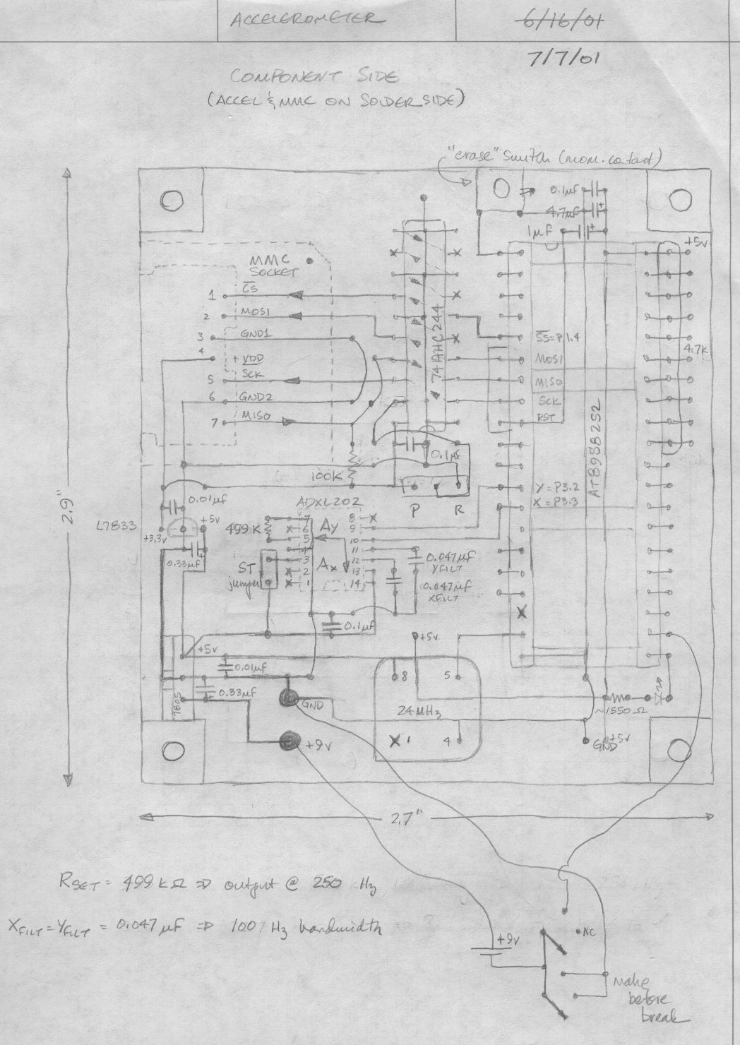
Below is a rough schematic of the layout
of the accelerometer PC board looking from the component
side. The microcontroller is an Atmel AT89S8252, an 8051
clone. This microcontroller is in-circuit programmable
using an SPI interface. The SPI pins are also used to
drive the MMC. To permit the dual use there is a jumper
block (located below the 74AHC244, marked "P" and "R")
that allows the pins to be connected for programming (P)
or running the code (R). Speaking of the 74AHC244 chip,
it MUST be the 74AHC family version. Regular old 74LS or
74HC etc. will not work, at least not for long. The AHC
family allows the chip to be powered by 3.3v yet will
not be destroyed by 5v inputs. It is used in this
circuit to allow the 5v microcontroller to talk to the
3.3v or so MMC. Without, hopefully, damaging anything.
Pins 31 through 40 of the microcontroller are connected
with a 4.7Kohm resistor pack. This effectively ties pins
31 through 40 to 5v. This was done so port 0 could be
used as I/O at a later date if desired and, more
importantly, to tie pin 31 high so the microcontroller
would work at all. If this resistor pack is left out,
pin 31 must still be held high some way.
The accelerometer itself is a surface
mount chip and is thus shown from the bottom on this
schematic as if you were looking through the board. The
same holds true for the MMC socket. The accelerometer
has an external resistor used to select the data rate
and external capacitors to smooth the output. The values
shown cause output at a theoretical 250 Hz with the bulk
of the signal beyond 100 Hz filtered out. In reality
this unit runs at 273 Hz. There is a jumper next to the
accelerometer that can be used to perform a self test. I
never used this feature but it's explained by the
accelerometer datasheet which is available from the
Analog Devices web site.
There are two linear power supplies on
this board. A 7805 at the lower left powers everything
except the MMC and 74AHC244. A 7833 shown above the 7805
drops the voltage further to power these two devices.
There are two switches on this unit. The
main switch, which runs to the outside of the box is
shown at the lower right. This is a two pole, three
position switch with the added feature that one pole is
closed in switch positions 2 and 3 while the other is
closed only in position 3. The leg that is closed in
positions 2 and 3 is the power switch for the device. It
is the intermediate position so when the switch is moved
from "off" to the first detent the unit powers up. It
immediately reads the address of the first empty memory
location in the MMC and then enters a loop and waits.
When the switch is then moved to the third position, the
second pole grounds an I/O pin on the microcontroller.
This signals it to leave the loop and start taking data.
When data collection is over, the switch is moved back
to the middle position. The microcontroller again
detects this, finish writing the current memory block,
stores the next memory address in block 1 then goes into
an endless loop until power is turned off.
The second switch is a momentary contact
switch located on the circuit board along the top edge.
This switch is used to "erase" the MMC. If it is held
down while the unit is powered up it will write the
address of "0000h" into the first block of the card. The
next time the unit is powered up normally it will thus
begin writing at the start of memory.
The only visual indication that data is
being taken is given through two LED's. A green LED
blinks about twice per second when the power switch is
in the intermediate position. This blinking occurs only
when the required reads/writes of block one are
completed to let the user know it's safe to proceed to
recording data or to turn the unit off. A red LED gives
one quick flash when the memory is "erased". It also
blinks if an error occurs. The number of flashes in each
sequence yields the error number which is halfway
documented in the assembly language routine.
The final component of note is the 24MHz
CMOS clock oscillator at the bottom of the schematic.
This speed was needed to keep up with the data rate
selected. In reality, the MMC sometimes takes a hair too
long to store a block of data causing a glitch in the
data. These usually occur about once a second and affect
one or two data points so I tend to ignore them rather
than try to fix them.
Click Here
to View Circuit
|
