|
A combinatorial circuit is a generalized
gate. In general such a circuit has m inputs and n
outputs.
Such a circuit can always be constructed as n separate
combinatorial circuits, each with exactly one output. For that
reason, some texts only discuss combinatorial circuits with exactly
one output. In reality, however, some important sharing of
intermediate signals may take place if the entire n-output
circuit is constructed at once. Such sharing can significantly
reduce the number of gates required to build the circuit.
When we build a combinatorial circuit from some kind of
specification, we always try to make it as good as possible.
The only problem is that the definition of "as good as possible" may
vary greatly. In some applications, we simply want to minimize the
number of gates (or the number of transistors, really). In other, we
might be interested in as short a delay (the time it takes
a signal to traverse the circuit) as possible, or in as low
power consumption as possible. In general, a mixture of such
criteria must be applied.
Circuit minimization is a difficult problem from complexity point
of view. Computer programs that try to optimize circuit design apply
a number of heuristics to improve speed. In this course, we
are not concerned with optimality. We are therefore only going to
discuss a simple method that works for all possible combinatorial
circuits (but that can waste large numbers of gates).
A separate single-output circuit is built for each output of the
combinatorial circuit.
Our simple method starts with the
truth table (or rather one of the acceptable truth tables,
in case we have a choice). Our circuit is going to be a two-layer
circuit. The first layer of the circuit will have at most 2n
nand-gates, each with n inputs (where n
is the number of inputs of the combinatorial circuit). The second
layer will have a single nand-gate with as many inputs as
there are gates in the first layer. For each line of the truth table
with an output value of 1, we put down a nand-gate
with n inputs. For each input entry in the table with a
1 in it, we connect an input of the nand-gate
to the corresponding input. For each entry in the table with a
0 in it, we connect an input of the nand-gate to the
corresponding input inverted.
The output of each nand-gate of the fist layer is then
connected to an input of the giant nand-gate of the second
layer. And that's it.
As an example of our general method, consider the following truth
table (where a - indicates that we don't care what
value is chosen):
  x y z | a b
  -----------
  0 0 0 | - 0
  0 0 1 | 1 1
  0 1 0 | 1 -
  0 1 1 | 0 0
  1 0 0 | 0 1
  1 0 1 | 0 -
  1 1 0 | - -
  1 1 1 | 1 0
The first step is to arbitrarily choose values for the undefined
outputs. With out simple method, the best solution is to choose a
0 for each such undefined output. We get this table:
  x y z | a b
  -----------
  0 0 0 | 0 0
  0 0 1 | 1 1
  0 1 0 | 1 0
  0 1 1 | 0 0
  1 0 0 | 0 1
  1 0 1 | 0 0
  1 1 0 | 0 0
  1 1 1 | 1 0
Now, we have to build two separate single-output circuits, one
for the a column and one for the b column.
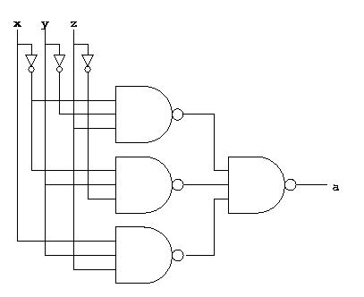
For the first column, we get three 3-input nand-gates in
the first layer, and a 3-input nand-gate in the second
layer. We get three nand-gates since there are three rows
in the a column with a value of 1. Each
one has 3-inputs since there are three inputs, x,
y, and z of the circuit. We get a 3-input
nand-gate in the second layer since there are three nand-gates
in the first layer.
Here is the complete circuit for the first column:
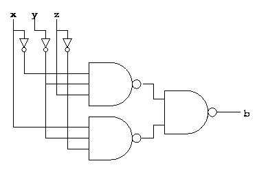
For the second column, we get two 3-input nand-gates in
the first layer, and a 2-input nand-gate in the second
layer. We get two nand-gates since there are two rows in
the b column with a value of 1. Each one
has 3-inputs since again there are three inputs, x,
y, and z of the circuit. We get a 2-input
nand-gate in the second layer since there are two nand-gates
in the first layer.
Here is the complete circuit for the second column:
Now, all we have to do is to combine the two circuits into a
single one:
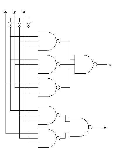
While this circuit works, it is not the one with the fewest
number of gates. In fact, since both output columns have a 1
in the row correspoding to the inputs 0 0 1, it is
clear that the gate for that row can be shared between the two
subcircuits:

In some cases, even smaller circuits can be obtained, if one is
willing to accept more layers (and thus a higher circuit delay).
|


